IMEC Outlines CMOS 2.0 Path As AI Compute Demand Rises
CommonWealth Magazine English reported that IMEC's new CEO Patrick Vandenameele outlined semiconductor roadmap work tied to AI inference demand, CMOS 2.0 stacking, memory placement and optical interconnects. CommonWealth reported that Vandenameele estimated a 150-fold workload increase as AI shifts from training to inference, while TSMC's Kevin Zhang pointed to nanosheet, CFET and 3D stacking work.
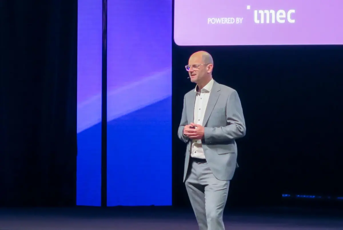
AI compute demand is pushing IMEC's roadmap toward CMOS 2.0 stacking, closer memory placement and optical interconnects, according to CommonWealth Magazine English.
At the ITF World summit in Antwerp, IMEC's new CEO Patrick Vandenameele outlined that work, the publication wrote.
The Belgium-based research institute works with companies including TSMC, Samsung, Intel and ASML, and its roadmap already extends into the early 2040s.
AI Inference Pushes Compute Demand
Vandenameele described AI growth as shifting from training toward multi-agentic systems, where dozens or hundreds of agents work together.
CommonWealth wrote that he estimated the move from training to inference will increase computing workloads 150-fold.
That hardware shift brings memory and logic chips closer together, the article noted.
It added that simply adding more GPUs is no longer the optimal approach because computing architecture must change.
CMOS 2.0 Extends Scaling Beyond 2nm
IMEC's CMOS 2.0 platform uses vertical transistor layers with different functions, joined by wafer-to-wafer hybrid bonding.
CommonWealth wrote that each layer is optimized for a different function.
Latest results from the research institute showed that even a two-layer stack improved energy efficiency.
In the roadmap cited by CommonWealth, shrinking chips from 2nm to 0.5nm together with CMOS 2.0 stacking could deliver a tenfold performance improvement over the next decade.
TSMC Co-Chief Operating Officer Kevin Zhang outlined a transistor architecture shift from FinFET to nanosheet, with CFET as the next step.
He added that transistor scaling, higher density and 3D stacking could increase transistor counts within a single package nearly 50-fold, while EDA tools remain a current obstacle for stacking logic chips.
Memory And Optical Links Move Into The Package
For memory architecture, IMEC placed high-bandwidth memory at the center of the compute module rather than at the chip edge.
Zhang also noted that TSMC is working with DRAM partners on technology that stacks DRAM directly on advanced logic chips.
CommonWealth cited Cerebras as an example of closer memory integration, writing that the company worked with TSMC to combine more than 50 compute chips on a single wafer with large amounts of high-speed SRAM to accelerate inference.
Public Evidence Still Stops At Roadmap Level
Vandenameele warned that copper cabling faces bandwidth and space limits as more chips are placed in racks.
IMEC's roadmap aims to move optical connections from between racks to within racks and eventually toward an optical highway inside the interposer.
The account did not name customer adopters for CMOS 2.0, disclose a commercial rollout schedule, or provide manufacturing dates for optical-interposer work.