SendTech Times
News
SUPPLY CHECK:

IBM Shows Sub-1 Nanometer Chip Research, With Production Proof Still Missing

Newsroom brief

IBM unveiled a 0.7 nm nanostack chip technology with nearly 100 billion transistors, but the company has not announced a manufacturing partner, production date or customer design win.
Verified against source materialEdited by SendTech Times Chips & Compute DeskSource: IBM Newsroom
IBM Shows Sub-1 Nanometer Chip Research, With Production Proof Still Missing
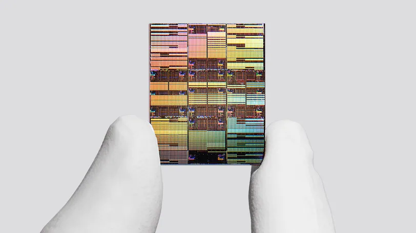
Image source: IBM Newsroom

IBM Pushes Chip Scaling Below One Nanometer

The account comes from an official company announcement and does not include independent customer validation, contract terms or deployment metrics.

The account is based on IBM research material; it does not include foundry production commitments, customer adoption or independent manufacturing validation.

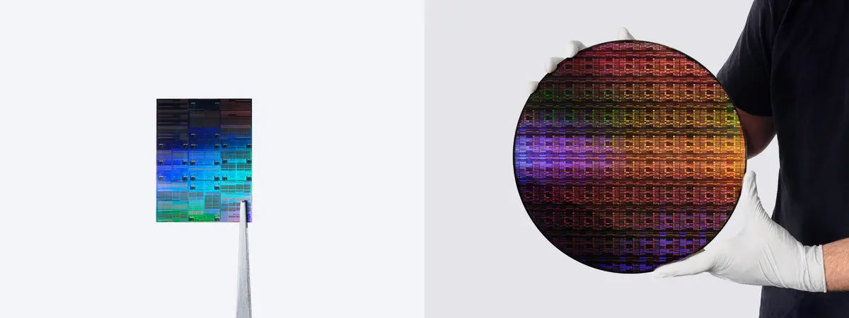
IBM has unveiled a sub-1 nanometer chip technology built around a three-dimensional nanostack transistor architecture, presenting the research as a way to extend semiconductor scaling as conventional designs approach atomic dimensions.

The company described the node as 0.7 nm, or 7 angstroms.

It said the research device reaches nearly 100 billion transistors on a fingernail-scale die, a density level IBM compared with the 2 nm chip it unveiled in 2021.

The research matters for AI compute because interconnect density, transistor scaling and power control affect future accelerator design.

IBM said it projected a performance gain of up to 50 percent, or a 70 percent energy-efficiency improvement, against its 2 nm node chips.

Those figures are research projections, not shipping product claims.

IBM also framed the advance as a response to the limits of traditional chip scaling.

The company said semiconductors are central to computing, appliances, communications devices, transportation systems and critical infrastructure, which makes any credible path to denser logic relevant beyond a single product line.

IBM did not announce a manufacturing partner, production date, foundry process transfer, first customer design or commercial chip family using the new architecture.

Nanostack Changes The Transistor Layout

IBM said nanostack is a three-dimensional, nanosheet-based design that vertically stacks and staggers transistors.

The design uses 3D sequential integration to increase transistor density and allows different material combinations within stacked layers.

The company said researchers had tested the architecture through CMOS integration work involving ultra-thin dielectric bonding, dual-channel engineering and functional inverter operation.

Those claims show that IBM is presenting the work as more than a drawing-board roadmap, while still keeping it in the research stage.

IBM also cited research presented at VLSI 2026 showing 40 percent scaling in SRAM.

That memory detail matters for advanced AI workloads because SRAM density and bandwidth shape how quickly chips can move data close to compute.

The design also gives IBM a materials argument.

By allowing different material combinations inside stacked layers, nanostack is meant to tune power efficiency and performance separately across parts of the transistor structure.

The public record still lacks which foundry process or supply chain would carry that materials work into commercial manufacturing.

AI Compute Still Needs A Commercial Path

IBM framed the work as a decade-long scaling path for logic technology below the 1 nm node.

It also connected the architecture to generative AI, cloud infrastructure and electronic devices that require higher performance per watt.

Jay Gambetta, director of IBM Research and an IBM Fellow, said the nanostack architecture is meant to reinvent how chips are built for more power and energy efficiency.IBM described the work as a platform-level research advance rather than

The timing also matters for customers planning AI infrastructure.

Better performance per watt can reduce pressure on data-center power budgets only if the technology reaches manufacturable chips with acceptable yield, cost and packaging support.

IBM's release does not provide those manufacturing economics.

The commercial burden remains outside the announcement.

IBM has technical validation, density targets and performance projections for sub-1 nm logic, but it has not named the factory, production schedule, chip customers or yield evidence needed to turn nanostack research into deployed AI compute.

Share this article
inXf

Related articles

More
IBM Claims Sub-1 Nanometre Chip Path With Production Still Five Years Away
Chips & Semiconductors

IBM Claims Sub-1 Nanometre Chip Path With Production Still Five Years Away

IBM says its nanostack architecture can put nearly 100 billion transistors on a fingernail-sized chip and move sub-1 nanometre technology into production within five years. The claim targets AI efficiency, but IBM has not named customers or manufacturing partners for the process.

Cerebras Plans 8x To 10x Manufacturing Scale-Up For AI Inference
Chips & Semiconductors

Cerebras Plans 8x To 10x Manufacturing Scale-Up For AI Inference

Cerebras chief executive Andrew Feldman said the company plans to scale manufacturing capacity by 8x to 10x this year and claimed its systems can run inference 10, 15, 20 or 30 times faster than GPUs. The interview-led source named customers including AlphaSense, Cognition AI, OpenAI, Block and GlaxoSmithKline, The public record still lacks third-party benchmark methodology.

LineShine Tops TOP500 Without Nvidia, Intel Or AMD Chips
Chips & Semiconductors

LineShine Tops TOP500 Without Nvidia, Intel Or AMD Chips

China’s LineShine supercomputer reached 2.198 Exaflop/s on the TOP500 list using local LX2 processors, but its Armv9 design and Linux base show that compute sovereignty still depends on global technology layers.

QIA Joins $380 Million Nearfield Round For AI Chip Metrology
Chips & Semiconductors

QIA Joins $380 Million Nearfield Round For AI Chip Metrology

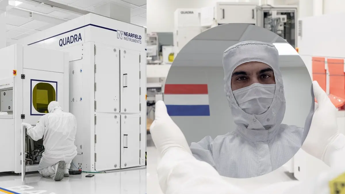
Nearfield Instruments raised $380 million at a $1.6 billion valuation, with Qatar Investment Authority joining a semiconductor metrology round aimed at advanced AI chip manufacturing.

Groq Raises $650 Million As Its AI Chip Story Turns Toward Neocloud Scale
Chips & Semiconductors

Groq Raises $650 Million As Its AI Chip Story Turns Toward Neocloud Scale

Groq announced a $650 million round after Nvidia licensed its technology and hired senior leaders, leaving the AI chip company to rebuild around a neocloud business spanning 13 data centers.

Micron Commits $10 Billion To Boise AI Memory Research Hub
Chips & Semiconductors

Micron Commits $10 Billion To Boise AI Memory Research Hub

Micron Technology is putting $10 billion into Micron Research Labs, a Boise research hub focused on advanced memory, compute architectures, packaging and semiconductor manufacturing for AI systems. The company expects to break ground in 2027.

ASRock Rack Shows 1U Arm AGI Server Before CPU Ramp
Chips & Semiconductors

ASRock Rack Shows 1U Arm AGI Server Before CPU Ramp

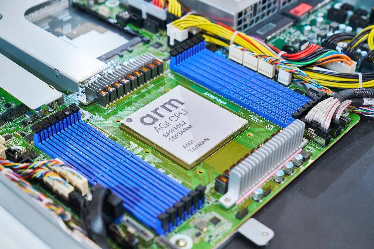
ASRock Rack displayed a 1U4E1S-ARM server for Arm’s AGI CPU at Computex 2026, with one processor, 136 Neoverse V3 cores and PCIe Gen6 connectivity, ServeTheHome reported. The report did not list pricing, customer deployments or a commercial launch date for the 1U system.

Onsemi Synaptics Deal Adds Edge AI Compute With Approval Still Pending
Chips & Semiconductors

Onsemi Synaptics Deal Adds Edge AI Compute With Approval Still Pending

Onsemi is buying Synaptics in an all-stock deal valued at about $7 billion to add edge AI compute, wireless connectivity and human-machine interface assets. The transaction is expected to close in mid-2027 if regulators approve it, but customer deployments and integration milestones remain undisclosed.

Keep Reading

More Stories

Latest
Kepler Targets 2027 Production for HBM Replacement MemoryCloud & Data CentersOct 6, 2026Kepler Targets 2027 Production for HBM Replacement MemoryEE Times reports that Kepler Computing is preparing 3D ferroelectric memory for 2027 production, promising higher capacity and bandwidth per watt while limiting reliance on advanced-node lithography.Yokogawa Opens Singapore Hub For Industrial Cyber ResilienceCapital & PolicyOct 6, 2026Yokogawa Opens Singapore Hub For Industrial Cyber ResilienceYokogawa Engineering Asia has launched a Singapore center focused on OT cyber resilience, training, response planning and recovery coordination for Southeast Asia, Oceania and Taiwan.ClickFix Attack Uses Browser Cache To Hide Malware PayloadCybersecurityOct 6, 2026ClickFix Attack Uses Browser Cache To Hide Malware PayloadMicrosoft Threat Intelligence traced a ClickFix cache-smuggling method that preloads malware into browser caches, then uses file size checks and a pasted Run command to launch later credential-theft stages.VOA Tests Six-Month Startup Buildout Before Funding DecisionsFintech & Digital PaymentsOct 6, 2026VOA Tests Six-Month Startup Buildout Before Funding DecisionsTechCabal’s interview with VOA Venture Partners founder Victoria Olayide Adesanya describes a six-month build programme that lets the firm work inside African financial-infrastructure startups before deciding whether to invest.Bitcoin Holds $86,000 As Dollar Index Hits 18-Month HighCrypto/Web3Oct 6, 2026Bitcoin Holds $86,000 As Dollar Index Hits 18-Month HighCoinDesk reported that bitcoin stayed near $86,000 while the U.S. Dollar Index reached about 102.5, with U.S. rate expectations and European political risks strengthening the dollar backdrop.Google Freezes OSS Bug Bounty Reports After AI Submission FloodCybersecurityOct 6, 2026Google Freezes OSS Bug Bounty Reports After AI Submission FloodGoogle has stopped accepting new product vulnerability reports in its OSS VRP after invalid automated submissions swamped reviewers, while older reports and some Cloud VRP routes remain open.Fleuret AI Raises €4M For Continuous AI Pentesting PlatformCybersecurityOct 6, 2026Fleuret AI Raises €4M For Continuous AI Pentesting PlatformTech.eu reported that French startup Fleuret AI raised €4 million in pre-seed funding to develop an agentic-AI platform that turns penetration testing into a continuous security process.GFT Analysis Says AI Documentation Can Cut Maintenance Work 30%Fintech & Digital PaymentsOct 6, 2026GFT Analysis Says AI Documentation Can Cut Maintenance Work 30%A GFT Technologies analysis says AI-linked software documentation can cut maintenance effort and speed developer onboarding when knowledge assets stay synchronized with code changes.Schneider Electric Lines Up $22.6 Billion PTC DealAIOct 5, 2026Schneider Electric Lines Up $22.6 Billion PTC DealSchneider Electric plans to buy PTC in a cash transaction valuing the US engineering software provider’s equity at about $22.6 billion, adding product-lifecycle software to its industrial AI push.Aggarwal Pledges Ola Electric Stake To Fund ₹1,000 Cr Rights IssueCapital & PolicyOct 5, 2026Aggarwal Pledges Ola Electric Stake To Fund ₹1,000 Cr Rights IssueOla Electric founder Bhavish Aggarwal pledged 20 Cr shares to finance his participation in a rights issue that forms part of a larger ₹1,500 Cr fundraising plan.Natrona Schools AI Review Puts Student Privacy Ahead Of Classroom Tool UseAIOct 5, 2026Natrona Schools AI Review Puts Student Privacy Ahead Of Classroom Tool UseNatrona County trustees questioned whether teacher AI tools expose student data, even as existing district rules already ban unauthorized generative AI use by students.AMD Prices 256-Core EPYC 9996 At $14,904 For Server BuyersChips & SemiconductorsOct 5, 2026AMD Prices 256-Core EPYC 9996 At $14,904 For Server BuyersTechRadar reports that AMD’s 6th Gen EPYC 9006 “Venice” lineup includes a 256-core EPYC 9996 with 512 threads, 1GB of L3 cache, a 600W default power rating and a $14,904 list price for 1,000-unit orders.