SK hynix Sets KRW 100 Trillion Cheongju Plan For NAND And Packaging
SK hynix said it will invest KRW 100 trillion in Cheongju for the M17 NAND fab and P&T7 packaging facility, while customers, order volumes and signed supply commitments remain outside the public record.
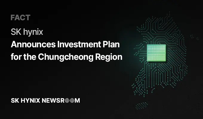
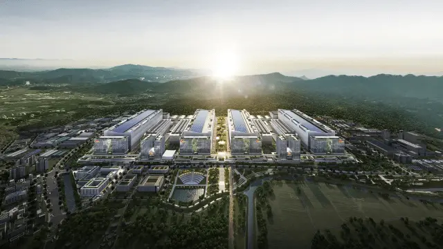
SK hynix plans to invest KRW 100 trillion in Cheongju, with KRW 80 trillion going to a new NAND fabrication plant and KRW 20 trillion to an advanced packaging facility.
The investment is designed to expand semiconductor capacity as artificial-intelligence services drive demand for enterprise SSDs, NAND flash memory, HBM and server DRAM.
The company announced the plan at a national briefing on next-generation advanced industries in the Chungcheong Region, held at Samsung Display’s Asan Campus in South Chungcheong Province.
President and CEO Kwak Noh-Jung said supply shortages and surging demand had made production expansion essential.
M17 and P&T7
The larger share of the investment will fund M17, a new NAND production fab in Cheongju.
Construction is scheduled to begin next year, with operations targeted for the first half of 2029.
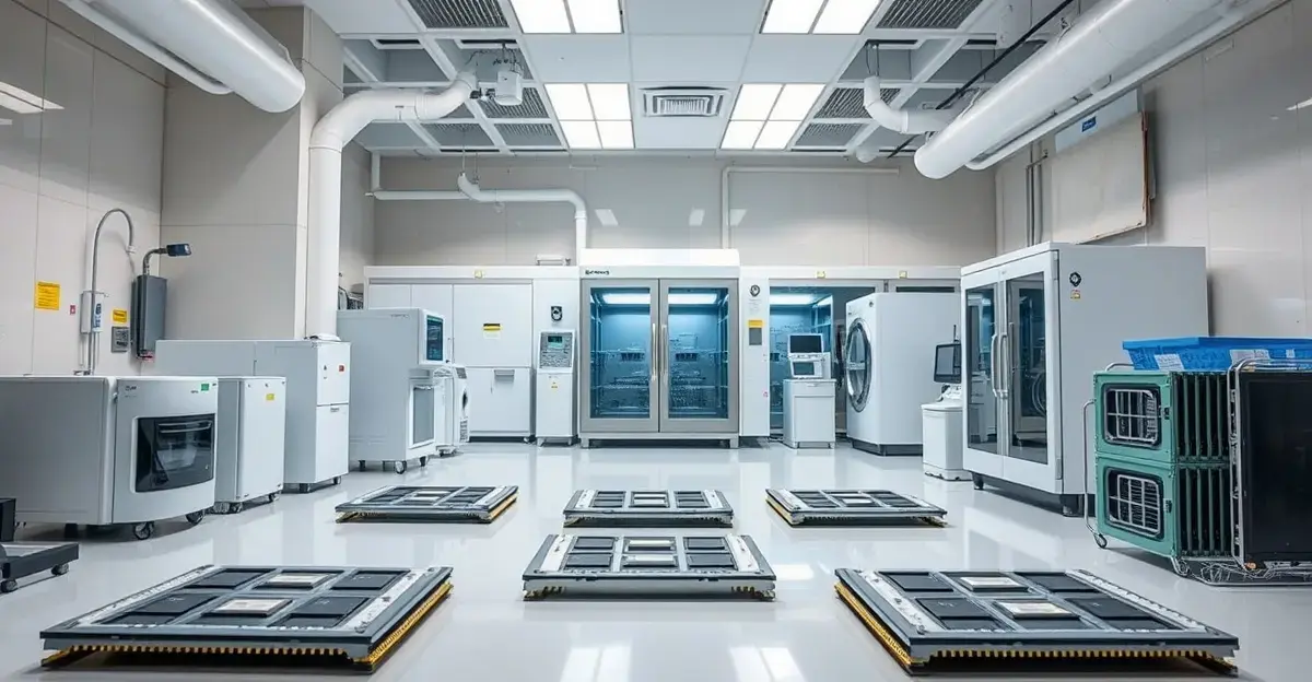
P&T7, the advanced packaging facility, is expected to be completed by the end of 2027.
SK hynix said the KRW 20 trillion allocation covers P&T7 and other facilities, while M17 accounts for approximately KRW 80 trillion.
The company is positioning the two projects as part of a broader memory-semiconductor expansion.
As AI adoption accelerates, demand is rising for enterprise SSDs and NAND flash memory alongside HBM and server DRAM.
SK hynix also expects agentic AI and physical AI to broaden the applications for NAND products and increase demand further.
Why Cheongju
Cheongju already has the land, electricity and water infrastructure needed for large-scale semiconductor construction, allowing work to proceed quickly.
The new fab can also coordinate production with SK hynix’s existing Cheongju facility.
Kwak described the city as the optimal site for rapid and efficient NAND expansion and said the investment would re-establish Cheongju as a key hub for Korea’s memory-semiconductor competitiveness.
The company plans to use its existing progress in NAND, HBM and advanced packaging in the Chungcheong Region as a base for further development.
A 1 GW AI data center
SK Group is pairing the semiconductor investment with a nationwide expansion of AI data-center infrastructure.
It plans to phase in 15 GW of capacity across South Korea, beginning with an initial 5 GW.
Within the Chungcheong Region, the group plans to build a 1 GW AI data center.
The project is intended to link semiconductor production with AI computing and help develop the region into what Kwak called a global center of AI semiconductor innovation.